Introduction
Semiconductor and IC packaging materials are at the heart of the technological revolution powering everything from smartphones to advanced computing platforms. As demand for miniaturization, improved performance, and sustainability increases, manufacturers and developers are challenged to innovate rapidly. Global advances in artificial intelligence (AI), edge computing, 5G networks, and high-performance devices are fueling a surge in the use and development of new packaging solutions. This article explores recent trends, leading industry players, global growth patterns, and notable country-wise developments shaping the industry’s trajectory.
Explosive Growth Expected
According to Straits Research, the global semiconductor & IC packaging materials market size was valued at USD40.34billion in 2024 and is expected to grow from USD44.11billion in 2025 to reach USD90.18billion by 2033, growing at a CAGR of 9.35% during the forecast period (2025-2033). This growth is driven primarily by the rising demand for compact consumer electronics, advanced computing devices, and the proliferation of digital infrastructure worldwide.
Key Trends and Technology Advancements
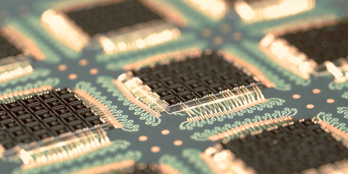
Shift to Advanced Packaging: The industry is transitioning from traditional packaging (like Dual In-Line Packages) to advanced solutions such as 2.5D/3D ICs, fan-out wafer-level packaging, chiplet integration, and system-in-package (SiP). These formats enable greater performance, density, and thermal management while facilitating high levels of device integration.
AI and Automation Integration: Artificial Intelligence is transforming production—automating tasks such as material selection, defect detection, and real-time process optimization. These advancements enhance manufacturing efficiency, accuracy, and yield, while reducing operational costs.
Drive for Miniaturization and Performance: Demand for smaller, more powerful consumer electronic devices (from wearables to smart home systems) continues to accelerate miniaturization and high-performance packaging solutions. Advanced materials such as novel polymers, underfills, and redistribution layers offer improved thermal conductivity, signal integrity, and mechanical resilience, supporting compact and feature-rich designs.
Growth in Data Center and HPC: High-performance computing and data centers are propelling the need for advanced thermal management and high-integration packaging formats. Segment growth is tied to the expansion of edge computing and the integration of AI technologies.
Leading Players and Recent Updates
Several major global players are spearheading innovation, efficiency, and investment in this sector. Companies such as ASE Technology Holding (Taiwan) have increased investments in advanced packaging foundries and high-density IC technologies. Amkor Technology (USA) expanded its microelectronics packaging operations and ramped up global production. GlobalFoundries (USA) recently unveiled a $575million center for chip packaging and photonics, further strengthening the country’s innovation landscape.
Japanese firms like Ajinomoto have committed to scaling up ABF film capacity by 2030. Meanwhile, Sumitomo Chemical (Japan) is enhancing capabilities in substrate insulation and packaging advancements. Samsung Electronics (South Korea) is focusing on 3D packaging breakthroughs and advanced memory solutions, while Intel (USA) is progressing with chiplet integration and next-gen formats. European and American companies, such as STMicroelectronics (Switzerland) and Advanced Micro Devices (USA), are broadening their offerings for automotive, IoT, and industrial markets.
Country-Wise Growth and Innovations
In the United States, government funding—such as the Department of Commerce’s $1.4billion initiative—is accelerating domestic capability in chip packaging and leadership. South Korea, fueled by Samsung and SK Hynix, is leading breakthroughs in high-bandwidth memory and 3D packaging solutions. Japan is experiencing renewed investment in robotics and interconnect packaging, while Taiwan holds a pivotal role as a frontrunner in 2.5D/3D and chiplet-based packaging development.
The European Union is backing growth with major public investment, driven by automotive, industrial, and smart device needs. These efforts focus on research and local supply chains. China remains a major force, rapidly advancing in consumer electronics, memory technologies, and R&D through robust government support and a dynamic domestic ecosystem.
The Role of 5G, IoT, and Automotive Electronics
Markets at the intersection of 5G, AI, IoT, and automotive electronics are sparking a boom of advanced packaging materials. The need to support faster data transmission, reduced latency, and enhanced miniaturization is amplifying demand, especially across Asia-Pacific, North America, and Europe. As 5G connections are projected to hit 1.8billion by 2025, companies with tailored packaging materials for next-generation devices are set to benefit enormously.
Key Challenges and Opportunities
Despite robust growth, manufacturers face challenges, including the higher cost of advanced technology, complex design requirements, and supply chain disruptions. The cost of adopting state-of-the-art materials is often 30–40% higher than with traditional solutions, creating hurdles for smaller entrants.
On the flip side, there are substantial opportunities in sustainable material technologies, recyclable solutions, and high-growth applications such as quantum devices, edge computing, and next-generation automotive systems.
Summary
The global semiconductor & IC packaging materials sector is entering an era marked by rapid innovation, strong investment, and diverse technological breakthroughs. With key players driving increased adoption of advanced packaging technologies and robust country-wise development, the future promises faster, smaller, and more powerful devices for a connected world.